|
||||
You may redistribute this newsletter for non-commercial purposes. For commercial use contact jack@ganssle.com. To subscribe or unsubscribe go here or drop Jack an email. |
||||
| Contents | ||||
| Editor's Notes | ||||
Tip for sending me email: My email filters are super aggressive. If you include the phrase "embedded muse" in the subject line your email will wend its weighty way to me. Aspencore has released their moderately-interesting "Mind of the Engineer" report. Some highlights:
You can get a free copy here. |
||||
| Quotes and Thoughts | ||||
Few fields have so large a gap between current best practices and average current practice – Fred Brooks |
||||
| Tools and Tips | ||||
Please submit clever ideas or thoughts about tools, techniques and resources you love or hate. Here are the tool reviews submitted in the past. |
||||
| Freebies and Discounts | ||||
Dale Magnuson won the LA104 mini logic analyzer in last month's giveaway. This month's giveaway is a BattLab-One current profiler from Bluebird-Labs.
Enter via this link. |
||||
| On the Cortex M ISA | ||||
In the last Muse I wrote about in-circuit emulators, a mostly defunct technology that was once central to this industry. Many readers sent in stories of their early development efforts and the tools they used. Some wandered far afield, commenting on processors they knew and loved. One that came up repeatedly was the PDP-11, Digital Equipment Corporation's wonderful 16 bit minicomputer. That was one of the first minis to have a totally orthogonal instruction set. In general, any instruction could use any addressing mode. It was a joy to code for. One of their main competitors, Data General, sold the Nova which was a much cheaper 16-bit mini. It's low cost was achieved in no small part to a lousy ISA where each instruction had its own modes. Their first offering in this series actually used a single 4-bit 74181 ALU and did 16 bit math one nibble at a time! How is the situation today? Pretty much all over the map. Some processors are throwbacks to the Nova. Others mirror the PDP-11 philosophy. Most of our work is in C/C++ today, and it's likely that many are only vaguely aware of what the hardware is doing. Let's look, briefly, at the now super-common Cortex M ISA, which is thoroughly modern and a really nice programming environment. What is muddling is that different Ms support different variants of the Thumb instruction set, where 16-bit instructions allow for better memory density. These parts come in many flavors, so I'll focus on some highlights. The Cortex M has sixteen 32-bit general purpose registers (there are a few other registers for interrupt control, the processor status word, etc.). R15 is the program counter, R14 the link register, and R13 is really two registers, being the main or process stack pointer. What does "link register" mean? There's no real CALL or RETURN instruction. Instead, one issues a BL instruction which jumps to a subroutine while placing the return address in R14. That mirrors the old Nova's way of calling functions where the JSR instruction place the return address in one of the four processor registers. It's fast, but for nested calls one must manage R14 manually. What's rather stunning is that many instructions are quite expressive. For instance, one can ADD.W Rd, Rn, Rm, shift, which implements:
         Rd = Rn + Rm(shifted by shift bits)
         (Rd, Rn and Rm represent registers)
Then there are the bit field instructions. For instance:
BFI.W Rd, Rn, #lsb, #width
... inserts <width> bits starting at <lsb> from register Rn to Rd That's pretty cool. Load instructions are pretty universal in processors and generally rather boring. The Cortex, though, has pretty sophisticated load and store instructions. For instance: LDM.W Rn, {Ra, Rb, Rx-Ry}
Loads registers Ra, Rb and Rx to Ry from memory starting at Rn. A lot of interesting permutations of this load/store exist. Likewise, the PUSH and POP instructions can move multiple registers on and off the stack. A DSP-like multiply and accumulate exists… but so does a multiply and subtract. MLS.W Rd, Rn, Ra implements: Rd = Ra – (Rd*Rn) UMLAL is a fancy 64 bit unsigned multiply and add. UMLAL.W Rdlo, Rdhi, Rn, Rm does: Rdhi, Rdlo = (Rn * Rm) + (Rdhi, Rdlo) Have you ever had to write code to reverse the bit order in a word? RBIT does that in a single instruction. TBB Rn, Rm ... jumps through a table of addresses, where Rn is the base of the table and Rm is an index into it. The processors support barrier instructions. Out of order execution means it's hard to know when something will happen. The DMB instruction insures all memory transactions prior to this instruction are complete, and DSB essentially halts further execution until every instruction prior to it has finished. Finally, many instructions permit a suffix that indicates whether or not the processor status flags should be updated. A pretty good reference is here. Joseph Yiu's The Definitive Guide to ARM Cortex-M3 and Cortex-M4 Processors and The Definitive Guide to ARM Cortex -M0 and Cortex-M0+ Processors are some of the best books for more info about these architectures. |
||||
| On Moore and Dennard | ||||
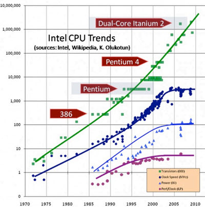
Moore's "Law" states that we can double the number of transistors every 18 to 24 months. Too many in the popular press, notably the New York Times' columnist Tom Friedman, think this is some sort of natural law that guides, well, everything. In fact, it was merely an observation made in the dinosaur era (1965) when few ICs had more than a hundred or so transistors. The "Law" became an aspiration as the semiconductor industry tried - successfully for many years - to shrink transistors to 0.7X their previous size every two years. (An IC, being two-dimensional, thus can have 1/(0.7 x 0.7), or about twice the number of transistors on the same size die). In 1974 Robert Dennard observed that as transistors shrink their power density stays roughly constant, so voltage and current scale proportionately. Since power is proportional to CFV2 we can get higher frequencies without burning up a chip. Thus: a cornucopia of goodness. More transistors, less power and higher clock rates. This is referred to as "Dennard Scaling". Like Moore's "Law" we can project into the future a zillion transistors operating at zetaHertz rates running from a single coin cell. Alas, like all things that are too good to be true, both Moore's "Law" and Dennard Scaling have met their maker. It has been years since anyone believed the semiconductor nodes promoted by the semi vendors. What does 7 nm really mean? That depends more on the marketing departments than the physicists. And Dennard Scaling failed around 2004 at about the 90 nm node. Dennard neglected leakage current and threshold voltage. Below a certain voltage transistors just don't work well (though a few vendors are now treading in this fearsome land. Eta Compute and Ambiq sell MCUs that operate below the threshold voltages, though at modest clock rates. And leakage current now contributes, by some estimates, as much as half the power used by high-end processors.
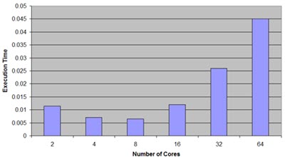
The death of Dennard Scaling So today we're maxed at around 4 GHz and a hundred or so watts. This is the reasoning behind multicore processors: you can't get much of a performance boost anymore by traditional methods like cranking up the clock rate, so distributing the work over more cores buys us better throughput. Alas, that may not always be true; Sandia National Labs has found that adding cores has a diminishing return:
Things are little different in the MCU world. Multicore does offer some serious benefits when we can assign work to a core that might be optimized for a particular task. For instance, an MCU might have a traditional von Neumann core coupled to a DSP. Or, it often makes sense to partition work between two or more von Neumann cores doing different things. Despite the failure of Moore/Dennard, I remain optimistic for the future of various kinds of IC scaling. Consider flash memory: Micron and others now offer 3-D flash. Micron manages to make it in 64 layers. They claim, as I understand it, to have true three dimensional silicon. The vendors are very parsimonious in their data and it's hard to learn much about how they make these parts. But cool? You bet. |
||||
| Eyes Wide Shut | ||||
A handful of emails that arrived over the last few months had a common theme. The short summary: These folks tried code inspections. They didn't work. I asked: How much code did you inspect? Answer: Uh, about 500 lines. Maybe 700. How did you do the inspection? Answer: We tested the code and found around 20-30 or so bugs. Perhaps more. Then we inspected and found another, well, maybe like 10 to 15. How long did debugging and inspecting take? Answer: We're not really sure but not too long. My response was this: The numbers are clearly meaningless. They're guesses. Unless you collect real metrics this data - such as it is - tells us nothing. How many bugs were left in the system? What makes you think you found them all? Do you know if you shipped with no bugs… or 100? Were the ones the inspection found mission-critical bugs? None of the folks had tried inspecting before debugging, making a murky situation even dimmer. We know that programming is different from building widgets on an assembly line. Yet too often people use that difference to excuse any attempt to measure and understand, quantitatively, the process of building firmware. A big part of engineering is measuring things, whether its amps, volts, miles/hour, furlongs per fortnight, or bug rates. Software engineering is engineering only when we collect real metrics, numbers like inspection efficiency, bug rates, productivity, and quality. There's a large body of knowledge about all of these subjects. If you don't collect your own metrics, there's no way to draw useful comparisons to the state of the art. That's like driving with your eyes shut. |
||||
| Failure of the Week | ||||
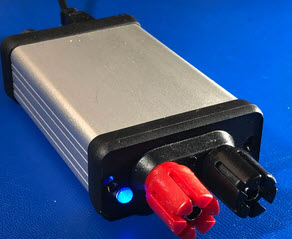
Steve O'Brien sent this:
|
||||
| Jobs! | ||||
Let me know if you’re hiring embedded engineers. No recruiters please, and I reserve the right to edit ads to fit the format and intent of this newsletter. Please keep it to 100 words. There is no charge for a job ad. |
||||
| Joke For The Week | ||||
These jokes are archived here. Any technology distinguishable from magic is insufficiently advanced. |
||||
| About The Embedded Muse | ||||
The Embedded Muse is Jack Ganssle's newsletter. Send complaints, comments, and contributions to me at jack@ganssle.com. The Embedded Muse is supported by The Ganssle Group, whose mission is to help embedded folks get better products to market faster. |