

By Jack Ganssle
Published July 30, 2010 in Embedded Systems Programming.
Power Management
The first decade of this century was surely a story of wireless connectivity. Billions of people now have cellular connections, and many have smart phones that - astonishingly - put the Internet into our pockets. 2010 saw the success of always-connected tablets, such as the iPad, and 2011 promises to see the release of a veritable zoo of similar products.
But the back story is more interesting and nuanced. These portable devices run for hours to weeks off batteries that make the proverbial cigarette pack look monstrous. Yet the CPU runs at hundreds of MHz, with tens of GBs of various forms of semiconductor memory. That half-pound phone has the compute horsepower of the recently-retired desktop rotting in your basement. The secret sauce behind portable electronics is the power management hardware and software, comprising hundreds of thousands of lines of code and big chunks of silicon.
Most microcontrollers today have at least a few power-saving sleep modes. But you will likely be surprised - shocked even - at the range of low-energy resources provided by the processors behind the portable connectivity revolution.
But first, a little background. Where does the power go?
Most of the energy supplied to a CPU is consumed in three different ways (there are some other current sinks but their importance is small). The first is driving I/O pins. A differential driver can take a fair amount of oomph, but in a typical connected mobile device the processor generally drives high impedance signals, and so these I/O lines represent a small portion of the energy used. The leakage and dynamic current requirements eat most of the power drawn by a processor. Leakage is just that: electrons that sneak through the silicon from power to ground. The effect is complex, but is proportional to the applied voltage and the intrinsic leakage of the material. The latter grows substantially as the transistor sizes shrink; in fact, it grows by about five orders of magnitude as the geometry goes from 250 nm to 65 nm. (http://www.altera.com/literature/wp/wp-01059-stratix-iv-40nm-power-management.pdf).
To make matters worse, leakage increases with temperature, to the tune of about an order of magnitude increase per 100�C (http://atrak.usc.edu/~massoud/Papers/IEICE-leakage-review-journal.pdf). The effect is an insidious feedback loop: the chip gets hot, so it leaks more, making it even hotter, all the while sucking ever more power. And that's the static dissipation, before the clocks are turned on, before the chip is doing anything useful.
With small geometries typically a third to a half of the power consumed is to leakage.
Dynamic current comes from charging the capacitive loads on the chip, since:

The dynamic power consumed by a processor is approximately:
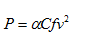
where C is capacitance, f is the clock frequency, v is the applied voltage, and a is the percentage of the circuit that switches with each clock transition.
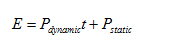
That formula is a little simplistic as it assumes the CPU is running at a constant speed all of the time. Since even simple microprocessors employ sleep modes it's more useful to think in terms of the amount of power consumed per work-item accomplished. If you have to do one thing, and then can shut the system down till there's something else needing attention, then the energy used per task is:
![]()
where t is the time spent accomplishing the task. Substituting:
![]()
Given that power is proportional to the voltage squared, it's critical to minimize V. Alas, lowering the voltage limits the maximum frequency attainable, which means the system must be out of a sleep mode longer to get a particular bit of work done.
To paraphrase that last sentence: is a constant for a given task. However, if the processor must be awake for more than doing one particular activity, cutting the clock frequency may be a better way to save power.
Most of us have programmed various sleep modes in our microcontrollers, and generally this is a pretty simple process. TI's MSP430 is touted as an "ultra-low power" controller, and indeed contains about 25 registers associated with setting and monitoring voltage levels (http://focus.ti.com/lit/ug/slau208h/slau208h.pdf). It provides about a half-dozen low power modes.
Microchip's eXtreme Low Power controllers such as the PIC16F1827 are also typical (http://ww1.microchip.com/downloads/en/DeviceDoc/41391C.pdf). The `1827 has a single very low power sleep mode controlled by a dozen registers, and its on-board peripherals may or may not be active during sleep.
Then there are the connected mobile device parts, which come with vastly more sophisticated power management features.
TI's OMAP 3530 is a part targeted to connected mobile devices and is an excellent example of a chip that offers a mind-bending array of power management capabilities.
It's far more than just a processor. The OMAP contains an ARM Cortex-A8 main CPU, a C64x DSP, a graphics accelerator, another processor to handle camera data, a display processor and a huge number of peripherals and peripheral controllers. It's a monster chip accompanied by a monstrous Technical Reference Manual (http://focus.ti.com/lit/ug/spruf98m/spruf98m.pdf), which is 3444 pages long. yet is woefully incomplete.
The part's Power, Reset and Clock Management (PRCM) component provides the resources needed to provide extended battery life to the user, and just this section consumes 400 pages of the TRM. By my count, 189 documented registers in the OMAP are dedicated to power management; there are actually more, but the additional ones are proprietary and are not in the public domain.
The OMAP 3530, like devices slated for similar applications, uses (among other things) clock and power gating to minimize power consumption. Remembering that the dynamic and static power together represent the bulk of the energy consumed by a device of this type:
![]()
But that assumes no sleep modes. With clock gating clocks going to portions of the chip that aren't needed get turned off (for instance, why power the USB interface when there's no comm going on?). For clock gating, the energy consumed by a particular portion of the chip during time t is:
That is, the energized component still draws static power even when clocks are off. Power gating removes the voltage to a component entirely:
![]()
And so the OMAP is portioned into a number of voltage, power and clock domains, with each one controllable via the software. Voltage domains are subsections of the chip powered by a particular voltage regulator. In fact, the OMAP doesn't like to play by itself; it really needs to be coupled to an external device like TI's TWL5030, which contains a dozen regulators, each of whose voltages are independently programmable via the firmware.
Since power used is proportional to the voltage squared, it pays off to get V to just the level needed. For instance, when listening to music little computation is going on, so it's possible to throttle the clocks down, and drop V to a lower value. Processing a camera image takes a lot of horsepower for a short period of time; V and F go to their max values. The voltage swing is tens of percent while clock frequencies can vary by over an order of magnitude.
Each voltage domain has a number of power domains, which further partition voltage distribution. The power domains enable or disable power to a subsection, or can in some cases put the subsection of the chip into a low-leakage retention mode. The eighteen different power domains include the wakeup logic, the MPU, the video processor, graphics engine, camera, USB, DPLLs, etc.
The alert EE's eyebrows may now be arched a bit. Turning power off to one part of a chip, which is connected to another, is a recipe for SCR latchup. But the chip automatically isolates connections to avoid this chip-destroying Armageddon.
Clock domains enable, disable and control clock rates to components within a power domain. The camera, for instance, has a number of clocks which can be turned on or off as required. There's no need to enable the serial communications clock to the image sensor when doing white balance adjustment, for example.
These hardware capabilities are combined with software to define Operating Performance Points (OPPs) which are typical combinations of clock frequencies and voltage levels. One OPP for high-performance needs might clock the ARM at 650 MHz, the DSP at 430 MHz, and set the voltage to those two components to 1.35. Simpler needs could define an OPP with 125/90 MHz clocks and 0.95 volt Vdd. The software sets registers to program the clocks, and sends USB commands to the external power controller chip to program the voltage regulators. This approach is referred to as Dynamic Voltage and Frequency Scaling (DVFS) and is quite common in the mobile world.
Clearly, these mobile devices offer a enormously fine-grained control of power consumption. In practice the OMAP may consume just a few milliamps or nearly an amp. Your mobile phone is constantly going through an exquisite ballet of modulated current consumption. But it's important to note that the concept of a global sleep or hibernation mode so often found on common processors doesn't really exist on the OMAP.
Then it starts getting complicated.
The weary firmware engineer must set up clock and power domain dependencies. That is, the OMAP lets one link domains together so, for instance, on a sleep or wakeup transition of one domain, other, linked domains will follow along as well. Clocks can be put in autoidle modes that shuts them down or enables them depending on other on-chip activities.
TI takes DVFS even further with their SmartReflex. This is a gestalt of the hardware resources noted above, extra undocumented hardware in the silicon, plus software that dynamically and automatically manages power to squeeze the most out of every electron drawn from the battery. It's very proprietary and secret but a paper (http://focus.ti.com/lit/wp/swpy015a/swpy015a.pdf ) gives some details. TI claims SmartReflex can reduce leakage current by three orders of magnitude using esoteric techniques that apply odd biases to "modulate the body voltage of transistor cells or blocks." I have no idea what that means or how it works, but it's clear there's an awful lot going on at the transistor level in the silicon.
Then there's battery management, which, in the case of the OMAP takes place either in the external TWL5030 power controller or yet another IC. Two general approaches are used - or, sometimes, both together. An A/D can monitor the battery's voltage, but that's a poor indicator of reserve capacity. Most batteries have a discharge curve with a rather sharp knee; pass the knee and the battery will rather suddenly run out of juice. Better is to measure amp-hours charged into the cell and withdrawn, and then apply corrections for battery temperature and aging. In fact, the TWL5030 companion chip also measures the battery's temperature, looks for over-voltage conditions, manages charging via a USB interface, and looks for over-current conditions. There's a lot going on!
This is but a simplified discussion of the OMAP's PRCM since the thing is bewilderingly complex. And there's a lot going on that TI won't divulge. I doubt that it's possible to actually use one of these parts without a lot of interaction with the vendor, but in the mobile world the volumes are so high that I'm sure vendors and customers form close engineering partnerships.
The world of power management is far bigger than the simple sleep modes we use on our smaller controllers. It's great for consumers who get devices that will run for days on a charge. I wonder if these techniques will find their way into other consumer appliances, like TVs, in the days ahead which promise perhaps significantly higher energy costs.