

Probing Pointers, or, Surprising Truths about Scope Probes
By Jack Ganssle
Derived from articles I wrote in Embedded Systems Design magazine and at embedded.com in March, April and May 2012. I also did two videos about this subject; one is Why Did My Board Crash When I Scoped a Node? The other is The Perils of Probing - What's Inside That Scope Probe.
Back when the Earth was starting to cool and the first creatures were crawling from the slime we were building a very fast system using plenty of discrete logic since the processors of those Paleozoic years couldn't keep up with our data rates. I was probing a pair of signals on a fabulously-expensive oscilloscope, but their relationship made no sense. Eventually I realized that one of the scope probe leads was a full meter longer than the other. This was the first, but certainly not the last, time I cursed light's snail-like pace. And it was the first time I was forced to think about scope probes, other than the routine of compensating them.
Eons later I still see engineers rooting around in a bin and untangling a random, often abused, probe, carelessly connecting it to the scope that they spent a week evaluating and comparing to a host of other products. But that $10k or $20k instrument (or more; I read a press release for a nifty $400k model recently) can be completely hobbled by a lousy or poorly-selected probe.
A scope probe is not a wire. Sure, it's an electrical connection between a node on a board and the oscilloscope. But its resistance, capacitance and inductance have serious consequences as speeds increase.
There are plenty of white papers that talk about proper probe selection, but to my knowledge none that show how the wrong probe can either cause your circuit to fail or even to physically destroy components. Let's look at some of the issues.
A lot of my readers are firmware folks without an EE, so here's a bit of background. There will be a little math, but fear not! Mostly this is as simple as Ohm's Law, which is:
![]()
E is voltage, I current, and R resistance. But there's really no such thing as a perfect resistor. Every component, be it a wire, resistor, or anything else has some amount of capacitance and inductance associated with it. So, while Ohm's Law holds true, as frequencies increase we need to include these effects in our thinking about resistance.
A capacitor passes AC but not DC, and the higher the frequency, or the larger the capacitance, the more easily it passes current. This is known as capacitive reactance, which is a form of resistance to alternating current. It's expressed as:
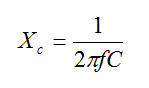
Reactance is in ohms since it "resists" electron flow. C is the capacitance in farads and f is the frequency in Hz. If f is zero - DC - the reactance is infinity and a perfect capacitor completely blocks current flow. As the signal gets faster it's reactance drops.
Inductors are similar:
![]()
In this case L is the inductance. So an inductor, too, has a resistive-like effect, though it is inverse of that of the capacitor.
If a circuit has inductance and capacitance, the total reactance is, well, it's thankfully not important to this discussion, but suffice to say that one can compute a net reactance. Toss in pure resistance and the total impedance - which is merely resistance to waveforms - in a parallel circuit is:
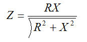
Z (impedance) is also in ohms, and is now a function of frequency.
Ohm's Law still holds, except we now replace R with Z. So it's possible to compute current flow in a complicated circuit at any given frequency if one knows the voltage and impedance.
I said there's no such thing as a perfect resistor. A typical 1/4 watt resistor has 0.5 pf of shunt capacitance. A wire-wound resistor is a coil and has inductance (though some have reverse windings to limit this). A normal film or carbon resistor has very little inductance.
A scope probe has capacitance, resistance and some inductance (mostly in that black ground wire), and looks something like this:
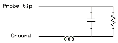
A scope probe, because of its impedance, is rather like a resistor that gets placed in parallel with the node you're testing. The net impedance of two in parallel is:
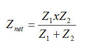
Thus, placing a probe on a node reduces the impedance of that point. Whatever drives the node must, in effect, push harder or the signal will degrade.
But is this really a big deal? Scope probes are typically specified at 10 million ohms, which is an enormous value. Put that in parallel with a digital device, whose resistance is orders of magnitudes lower, and there will be no measurable effect.
But what's important is impedance, not resistance, and as noted earlier, impedance depends on frequency. If you're probing a digital circuit odds are that things are switching pretty quickly. The frequency may be quite high.
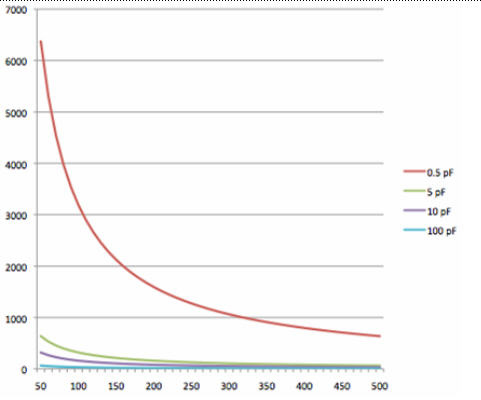
That's where the second part of a probe's spec, the tip capacitance, comes in. This ranges from under a pF to 100 pF or more. And that has a huge effect on the probe's impedance. Tektronix is one of the few vendors that gives graphs of probe impedance. Their TPP1000, a 1 GHz passive probe, has the following impedance vs. frequency curve:
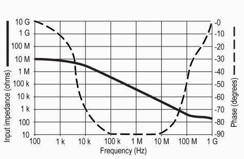
At 100 MHz the impedance appears to be around 500 ohms. The probe's capacitance is 4 pF; running the reactance numbers we get 400 ohms at that frequency, pretty darn close. At low frequencies the reactance gets very large so the 10 MΩ resistor dominates.
| Suggestion: Subscribe to my free newsletter which often covers scopes and logic analyzers. |
This is a $900 probe. Cheap probes may be considerably worse. The capacitance of Pomona's $117 5812A, rated for 300 MHz, is listed as "<17 pF." Let's assume 17. That's 93 ohms at 100 MHz. In a 5 volt circuit the probe will add a 54 ma load.
Surfing the net one finds lots of cheapies at 100 pF or worse, which nets a terrifying 20 ohms at 100 MHz. To put that into perspective, in a 2 volt circuit it would take 100 ma to drive the probe alone, and few gates can do that. Even at 10 MHz we're talking 10 ma. 74HCT gates, for instance, are generally rated at 4 ma. Other parts, notably processors, may be capable of driving less current. TI's OMAP35xx parts are spec'd at 2 ma on most pins.
The following chart shows the impedance of probes with 5, 10 and 50 pF tip capacitances:
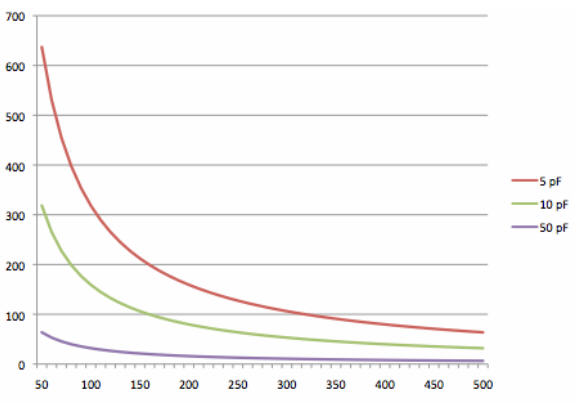
Let's do a little more analysis. Agilent's N2873A is a $400 good-quality probe with 9.5 pF tip capacitance. When connected to a 100 MHz signal it has 159 ohms of impedance. Looking at the 74AUC08 gate specification one finds that with a 2.3 volt supply the device can onlydrive 9 mA, yet a 159 ohm load demands 14 mA! At 0.8 V the situation is even worse; the gate can only supply about a tenth of the load needed by a probe.
In other words, connect one of these puppies to your board and the circuit may very well stop working. I think some of those homeless people I see in Baltimore are engineers who cracked when they found their troubleshooting tools made troubleshooting impossible.
Agilent has a really nifty 33 GHz scope. A high-quality probe like the $900 TPP1000 mentioned earlier will look like a one ohm load at that speed - the probe alone will draw over 2 amps at 2.3 volts! Thankfully the company sells much better probes. Though they do cost $30k each.
The important take-away is this: when buying a probe don't be seduced by the 10 MΩ rating. Think impedance, which is related to tip capacitance.
(A side note for those working with analog. Generally analog signals aren't as fast as digital so the probe-loading issues may be less severe. On the other hand, many analog nodes have a much higher impedance than digital. Even at DC putting a 10 MΩ probe across a 10 MΩ node will zap half the signal).
Better probes exist. Tek's 4 GHz P7240 has a tip capacitance of only 0.85 pF. Running the numbers we get 2 KΩ at 100 MHz, which exactly matches the chart in the device's manual. But this is an active probe, one loaded with electronics, and it'll set you back $5k. Which explains the sign held aloft by one gaunt street person last week: "Please help. Will work for a pair of P7240s."
Fourier Fits
But it gets worse.
In 1822 Joseph Fourier released his Theorie analytique de la chaleur (The Analytic Theory of heat). That seminal work has tormented generations of electrical engineering students (and no doubt others). Discontinuous functions - like square waves - are very resistant to mathematical analysis with calculus unless one does horrible things like use unit step functions. But Fourier showed that one can represent many of these periodic functions as the sum of sine waves of different amplitudes and frequencies. The Fourier Series for a square wave is:

The series goes on forever, so all square waves have frequency components going to infinity. However, the amplitude of these decrease rapidly due to the division by an ever-larger odd number. The point, though, is that the "frequency" of a square wave is composed of many frequencies higher than that of the baseband.
Pulses, like the ones that race around every digital board, the ones we probe with our scopes and logic analyzers, are square-wave-ish. The good news is that they are not perfect square waves: obviously, with the exception of clocks, they rarely have a 50% duty cycle. Pulses are also, happily, imperfect. Fourier's analysis assumed that the signal transitions between zero and one instantaneously. In the real world every pulse has a finite rise and fall time. If Tr is the rise time, then frequency components above F in the following formula will be so far down they're not important:

This does mean that, assuming a 1 nsec rise time, even if your clock is ticking along at a leisurely rate about the same as a Florida old-timer's speedometer, the signals have significant frequencies up to 500 MHz.
Those unseen but very real frequency components will interact with the scope probe.
Ad Hoc Formulas
Long troubleshooting sessions often see a board covered with connections to test equipment, data loggers, etc. Long lengths of wire-wrap wire get soldered between a node and an instrument. These connections all change the AC properties of the nodes by adding inductance and capacitance. Here are some useful formulas with which one can estimate the effects. These are derived from reference 1, and there's much more useful data in that book.
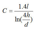
Most of us use multilayer PCBs that have one or more ground and power planes. Solder a wire to a node and drape it across the board as it runs to a scope or other instrument, and you'll add capacitance. If d is the diameter of the wire in inches, h is the height above the PCB, and l is the length of the wire, then the capacitance in pF is:
(A better solution is to run the wire straight up from the node, perpendicular to the PCB).
AWG 30 wire-wrap wire is 0.0124 inches in diameter. Typical hook-up wires are AWG 20 (0.036"), AWG 22 (0.028") and AWG 24 (0.022").
The inductance of the same wire in nanohenries is:
The inductance of a round loop of wire (for example a scope probe's ground lead) in nH is, if d is the diameter of the wire and x is the diameter of the loop:
Some Experiments
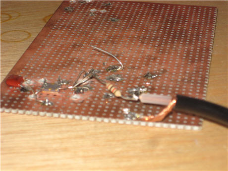
While Missouri may be the "show me" state, most engineers also want to see real-world demonstrations to prove a point. So I built a circuit on a PCB with ground and power planes, keeping all wires very short. A 50 MHz oscillator drives two AND gates. The 74AUC08 is spec'd with a propagation delay between 0.2 and 1.6 nsec at the 2.5 volts I used for the experiment. The second gate is a slower 74LVC08 whose propagation delay is 0.7 to 4.4 nsec. Still speedy, but slower than the first gate. I was not able to find rise time specifications, but assumed the faster AUC would switch with more alacrity, and thought it was be interesting to compare effects with differing rise times. Alas, it was not to be; the LVC wasn't much slower than the UAC. So I'll generally report on the slower gate's results
These parts are in miniscule SOT-23 packages which keeps inductances very low, but means one solders under a microscope, sans coffee.
I wanted to see the effect that probes have on nodes, but that posed a meta-problem: if probing causes distortion, how can one see the undistorted signal? Thankfully there's a simple solution derived from reference 1. I made a pair of meter-long probes from RG-58/U coax cable. A BNC connector on one end goes to the scope. A short bit of braid is exposed and soldered to the ground plane very close to the node being probed, and a 1/4 watt 1K resistor goes from the inner conductor to the node. Two views follow:
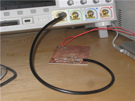
I used an Agilent MSO-X-3054A scope with selectable input impedance, set to 50 ohms as shown:
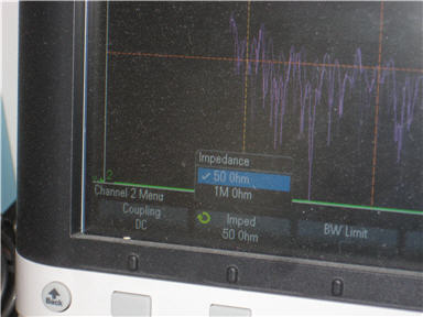
This is critical for the shop-made probe; the normal 1 MΩ simply will not work. If your scope doesn't have a 50Ω mode use a series attenuator such as the 120082 from Test Products International (this part doesn't seem to be on their web page, but Digikey resells them). Agilent's N5442A is a more expensive but better- quality alternative.
RG/58U is 50Ω cable; add the resistor and the total is 1050 ohms. The scope's 50Ω input forms a 21:1 divider, but the resistor's very low capacitance (remember, a 1/4 watt resistor runs only 0.5 pf) means the probe's tip looks extremely resistive, with little reactance. The scope thinks a 1X probe is installed, so to accommodate the oddball 21:1 ratio one multiplies the displayed readings by 21. Look at the phenomenal behavior of this probe (the red curve):
The first experiment showed Fourier at work. The blue trace in following figure shows the output of the fastest gate using a 21X probe. Note that it's far from perfect since the circuit had its own reactive properties. The rise time (measured with a faster sweep rate than shown) is about 690 psec (picoseconds). "About" is the operative word, as the scope has a 500 MHz bandwidth (though samples at 4 GS/sec). I found that having the instrument average readings over 128 samples gave very consistent results.
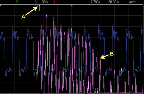
The pink trace is the Fourier Transform of the gate's output. Unlike the blue trace, this one is not in the time domain (e.g., time across the horizontal axis), but is in the frequency domain. From left to right spans 2 GHz, with 500 MHz at the center. The vertical axis is dBm, so is a log scale. Each peak corresponds to a term in the Fourier series. Point "A" is exactly 50 MHz, the frequency of the oscillator. Most of the energy is concentrated there. Peak "B" is 48 dBm down from "A." That's on the order of 100,000 times lower than "A."
"B" is at 900 MHz. Remembering that little energy remains in frequencies above ![]() ; with F=900 MHz the rise time is 555 psec, close enough to the 690 measured. The same experiment using the slower 74LVC08 gate yielded 48 dBm down at 450 MHz, or a rise time of 1.1 nsec. That's close to the 0.95 nsec reported by the scope.
; with F=900 MHz the rise time is 555 psec, close enough to the 690 measured. The same experiment using the slower 74LVC08 gate yielded 48 dBm down at 450 MHz, or a rise time of 1.1 nsec. That's close to the 0.95 nsec reported by the scope.
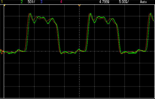
Next, I connected a decent-quality $200 Agilent N2890A 500 MHz probe (11 pf tip capacitance) on the 74LVC08's output. The 21X probe saw an additional third of a nanosecond in rise time due to the N2890A's capacitance. In other words, connect a probe and the circuit's behavior changes.
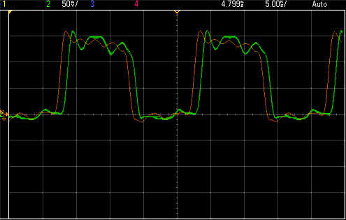
In the next figure the orange trace is the gate's output measured, as usual, with the 21X probe, although now there's 10" of wire dangling from it. That trace is stored as a reference, and the green one is the same point, with the same probe, but the N2890A is connected to the end of that 10" of wire. Note that the waveform has changed - even though that other probe is almost a foot away - and the signal is slightly delayed. This is probably not going to cause much trouble.
Gates typically have a very low output impedance, so it's unsurprising there's so little effect. Often, though, we're sensing signals that go to more than one place. For instance, the "read" control line probably goes from the CPU to quite a few spots on the board. To explore this situation I put the 21X probe five inches down that wire, captured the waveform into the reference (orange in the following figure), and then connected the same N2890A at the end of the 10" of wire. The signal (green) at the 5" point shifted right and was distorted as follows:
Consider the clock signal: on a typical board it runs all over the place. The impedance at the driver is very low, but the long PCB track will have a varying reactance. Probe it and the distortion can be enough to cause the system to fail.
The ringing is caused by an impedance mismatch. The N2890A has changed the node's impedance, so it no long matches that of the driver. Part of the signal is reflected back to the driver, and this reflection is the bounciness on the top and bottom of the pulses.
I didn't have any X1 probes around, so put a 100 pf capacitor on the node to simulate a really crappy probe. Rise time spiked to 5.5 nsec, more than a five times increase, and the signal was delayed by almost a nsec. I suggest immediately combing your lab for X1 probes and donating them to Goodwill. And be very wary of ad hoc connections - like clip leads and soldered-in wires - whose properties you haven't profiled.
But 100 pf is a really crummy probe. I soldered a 30 pf cap on the node to simulate one that's somewhat like an ad hoc connection or a moderately-cheap probe. In the next figure the orange trace is the gate's output with no load - just the 21X probe. The green is with the additional 30 pf. The distortion is significant.
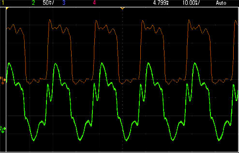
So a 30 pf probe grossly reshapes the node's signal. What effects could that cause?
First, everything this signal goes to will see a corrupt input. If it goes to a flip flop's clock input the altered rise time could cause data to be incorrectly latched. Or, if the flop's data input(s) are changing at roughly the same time, the flop's output could become metastable - it'll oscillate for a short time and then settle to a random value.
If it goes to a processor's non-maskable interrupt input the leading-edge bounce could cause the CPU to execute two or more interrupts rather than one. (Generally this is not a problem for normal maskable interrupts since the first one disables any others).
But wait, there's more. Note that the signal extends from well below ground (about -600 mV) to 3.7 volts (be sure to factor in the attenuation of the 21X probe), which is much higher than the 2.5 volt Vcc. Depending on the logic family this signal goes to, those values could exceed the absolute maximum ratings. It's possible the driven device will go into SCR latchup, where it internally tries to connect power to ground, destroying the device. I have seen this happen: the chips explode. Really. It's cool.
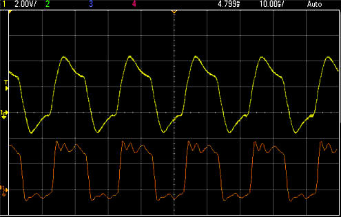
So far I haven't shown any signals acquired by the N2890A. The yellow trace in the next picture is the gate's output using that probe. It's pretty ugly! The distortion is entirely in the probe, and not on the board, so does not represent the signal's true shape. In this case the probe is grounded using the normal 3" clip lead. Using the formula from last month, that loop has 61 nH of inductance.
In orange the same signal is displayed, but in this case I removed the probe's grabber and connected a very short, about 5 mm, ground wire to the metal band that encircles the tip. The signal is still not displayed correctly - it extends below ground and has a total magnitude of about four volts, much more than the 2.5 Vcc. But the better grounding did clean up the shape. The point is that poor grounding can cause the scope to display waveforms that don't reflect the node's real state.
Conclusion
Many in the digital world find themselves divorced from electronics. We think in ones and zeroes, simple ideas that brook little subtlety. A one is a one, a zero a zero, and in between is a no-man's land as imponderable as the "space" that separates universes in the multiverse.
But electronics remains hugely important to digital people. Ignore it at your peril. Power supplies have crawled below a volt so the margin between a one and a zero is ever-tighter. On some parts the power supply must be held ±0.06 volts or the vendor makes no promises about correct operation. On a 74AUC08, typical fast logic, at 0.8 Vcc there's only a quarter volt between a high and a low. Improper probing can easily skew the node's behavior by that much. And, as we've seen, capacitance and inductance are so vital to digital engineering that we dare not ignore their effects when troubleshooting.
Reactance, impedance, and electromagnetics are big subjects that I've only lightly touched on. They're pretty interesting, too! I highly recommend the book cited in reference 1 for a deep and dirty look at working with high speed systems. Reference 2 is possibly the best introduction to electronics available. It doesn't skimp on the math, but never goes beyond complex numbers. The focus is decidedly on radios, since this is the bible of ham radio, but the basics of electronics are covered here better than any other book I've found. There's a new edition every year; my dad bought me a copy in 1966, and since then I've "upgraded" every decade or so.
Reference 1: High-Speed Digital Design by Howard Johnson and Martin Graham. 1993 PTR Prentice-Hall Inc, Englewood Cliffs, NJ.
Reference 2: The ARRL Handbook, American Radio Relay League. Published afresh every year.