

Quirky Chips
Originally published in Embedded Systems Design magazine in February, 2012.
There have been some really odd microprocessors over the last 40 years. Let's look at a couple.
Motorola's MC14500
64 bit CPUs and VLIW architectures slam massive amounts of data around via wide parallel busses. Processors today are so fast and so hungry for data that chip designers do horrible things to push bits into the CPU as quickly as possible. But at one time a narrow bus was seen as a competitive advantage.
Motorola's MC14500 was a one-bit CPU the company called an "Industrial Control Unit." The device's handbook has the intriguing statement "When a job is dominated by calculations or data logging, a multi-bit processor is appropriate. When the task is decision and command oriented, a one-bit machine is an excellent choice."
I can't determine when the chip came to market, but the handbook is dated 1977. Revision 3 of the datasheet was released in early 1994, so these odd devices did gain some traction. Rumor has it they were used in some HVAC systems and in a lot of ladder-logic applications. Indeed, the part's handbook goes on at great length about implementing ladders in MC14500 assembly language.
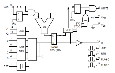
This was a very early Harvard architecture part in that there were two busses: one four bits wide for instructions, and a single-bit data bus. So though the "one-bit" moniker is somewhat correct, the device was a bit schizophrenic.
The MC14500's sixteen instructions did not include any arithmetic operations. No add, subtract, or the like. Instead, it included some simple loads and stores, ANDs and ORs, a jump, a single conditional skip, and a few instructions to control hardware. (It is possible to do arithmetic using just logical instructions).
Only a single register - the Results Register - existed, and that was, of course, just a bit wide.
This part was so quirky it didn't have a program counter. Designers were expected to create one external to the CPU. It's width was, well, anything the developer wanted. Running a tiny bit of code? Maybe an 8 bit PC was appropriate. Or 32 bits for those applications needing 4 GN (giga-nibbles) of powerhouse processing.
So the inevitable question is "how did a jump work?" That was entirely up to the engineer crafting the circuits. The OEN instruction could be used to disable any changes occurring on the output data; at the end of a loop assert OEN and let the machine execute whatever instructions - hopefully NOPs - remained until the PC rolled over. There was a JMP, but that instruction simply toggled an output bit. The design engineer was supposed to make that signal do something useful, like load the PC with some address.
As they would say here in Finksburg: "them boys at Motorola musta been smokin' somethin' illegal."
(The MC14500B's data sheet can be found here , and the part's handbook is here.)
RCA's 1802
RCA had been selling a processor using a pair of chips, but in 1976 they merged the two onto a single die. The 1802 is apparently still available, now from Intersil.
Not nearly as quirky as the MC14500, the 1802 had a pretty conventional architecture. In fact, with sixteen registers this 8 bit device was in some ways an improvement over contemporary parts. Each was sixteen bits wide in an era when competing CPUs had a few 8 bit registers and maybe a couple of special-purpose wider ones for indexing. The Z80, for instance, had a pair of 16 bit index registers, and a clumsy way to gang some of the byte-wide registers in pairs.
Handling so many registers with an 8 bit instruction was problematic, so the 1802 had several four bit pointer registers. Instructions indexed into the register set via these, and there were a slew of instructions used to load, store and otherwise manipulate the pointers. So, for example, an OR would combine the register indicated by the X pointer with the accumulator, annoyingly named "D," presumably for "Data." And, yes, the mnemonic for the Set X instruction was exactly what you're thinking.
Any of the 16 registers could be the program counter, which implies that one could do all sorts of interesting math on the PC. That made table-dispatching quite simple, and not a few developers wrote code so that data on an input port could immediately cause a change in control.
Lots of short branches were provided, but they were somewhat odd. Usually these sorts of instructions allow jumping from the PC plus or minus a certain amount (say, 127 bytes ahead or back). On the 1802 the short branches just loaded the low byte of the PC with a new value, so the range of the branch varied depending on where the instruction was in memory. Patch in a few instructions and it was possible you'd have a lot of rewriting to do as succeeding branches could no longer reach their destinations.
But one branch did not exist. There was no call instruction so a variety of tricks were used to invoke subroutines. When a program had only a handful of subroutines it was very efficient to assign a register to be each procedure's PC; other, rather clunky, approaches were used for bigger code bases.
Today we draw a pretty strong line between CPUs and microcontrollers. The former are naked processors while the latter include some mix of I/O and memory. The 1802 had a little built-in I/O which was not called such. Four "EF" pins and one "Q" were parallel I/O ports, and dedicated branch instructions sampled these.
It's a little hard to believe today, but once MOS logic was considered a poor substitute for bipolar, as it was very slow. RCA was an early MOS pioneer and had a popular line of logic called the CD4000 series. What the technology did give was a wide voltage range and astonishingly low power requirements. In the 70s the bipolar people (uh, those who were not bipolar) were straight-jacketed into slavish obedience to 5 volts with little tolerance for deviation. The 1802, being MOS (RCA called it COSMOS, latter shortened to CMOS) tolerated a wide Vcc range. That, plus the low power, made it ideal for battery-operated applications.
To further cripple the 1802's speed, it used at least 16 clock cycles per instruction.
1802s were widely used in space since it was one of the first rad-hardened microprocessors available. And at the bottom of the ocean; we used 1802s in deep sea probes that had to run for months on a few AAs.
Signetic's 8X300
In the mid-70s Scientific Micro Systems developed a part they called the SMS300, which Signetics manufactured. Eventually Signetics bought the rights to the device and renamed it the 8X300. It was sort of a predecessor to the DSP, and, being built with bipolar Schottky transistors, was very fast for the time. The datasheet (http://datasheets.chipdb.org/Signetics/8X300/8X300_1977.pdf) pegs the operating speed at a blistering 8 MHz, resulting in a 250 nsec instruction time. Yet to achieve that memory accesses could not exceed 65 nsec.
For reasons that completely elude me Signetics called the 8X300 a "microcontroller," yet there was neither memory nor I/O on-board. At one point the datasheet refers to it as an "interpreter."
The first bit of strangeness was the package, an enormous 50 pin DIP (old-timers will remember the first 68000 which was in an equally-huge 64 pin DIP). That allowed for separate instruction and data busses, and some claim that this was the first micro with a Harvard architecture. Instructions were 16 bits, with 13 address bits, and the data bus was just a byte wide.
It gets odder. The data bus was called the "Interface Vector bus," or IV for short, and bit 7 was the LSB! IV0 to IV7 were multiplexed with both address and data, suggesting that 256 bytes of data were supported. But, no, Left Bank and Right Bank signals selected one of two data sources, doubling the space. The nomenclature reminds me of Paris.
The data space included both RAM and I/O, and the latter was memory mapped.
The 8X300 contained a variety of registers, numbered R1 to R6 and R11. What about the missing ones? The numbers were the octal address of each register, and R11 for unknown reasons was at O11. R10, or at least the "register" at O10, was a one bit overflow flag, the only conditional bit. Only the ADD instruction could set or clear that bit. And R7 didn't really exist; it was a trick used to access the IV bus.
To read or write in data space or a register, one, well, the process is rather mind-boggling and there simply isn't enough room to describe it here. But the MOVE, ADD, AND and XOR instructions included fields to specify how many bits to rotate an argument. Except that sometimes those bits selected a field length.
There were four other instructions, including XEC, which executed the instruction pointed to by a bit of convoluted math. The PC pointed to the location after the XEC, unless the instruction executed was a jump. Strange, but it did make handling jump tables easy.
Note what's missing: there were no interrupts. No stack, no calls. And no subtract. But that was easy enough to simulate by taking the one's complement of the subtrahend, adding one to make the two's complement, and then adding the minuend. Each subtract consumed five instructions.
And Many More!
A number of microprocessors had quirky features that could be a curse or a blessing.
For example, the 4004 had a hardware stack, on-board the chip. It was three levels deep. That doesn't permit much subroutine nesting. Intel improved this on the 8008, making the stack seven levels deep. Even in those early days we tried to practice modular programming, so it was common to blow the stack via too many calls. The PIC1650 is often credited as being the first microcontroller (though I suspect the Scottish PICO1 probably deserves that honor). That part's stack was two deep, mirroring the similar PIC10 parts still selling today.
Interrupt cycles on Intel's 8080 were exactly like any fetch, except the CPU asserted an interrupt acknowledge pin. The hardware was then supposed to jam an instruction on the bus to vector to a handler. Eight one-byte calls (RST0-7) were provided for this purpose. But there were plenty of designs that used crafty logic to jam a three byte call. Where I worked we had severe time constraints and none of those approaches were fast enough due to the stack pushes involved. Instead, when awaiting a particular event, we'd branch to the handler and execute a halt instruction. The interrupt hardware would jam a NOP, which was the fastest instruction the CPU could execute, and the code following the halt, the interrupt handler, would resume.
For a while bit-slice processors were the rage for high-performance systems. The most popular was AMD's 2900 series. These four-bit slices could be cascaded together to build a system of any word length. Each chip had an ALU, a decoder for the eight instructions, and 16 nibbles of dual-ported RAM that acted as registers. Things like a program counter and the other components of a computer had to be added externally. Intel was in that game, too, with their 3000-series of two bit slices. Needless to say, a processor with a wide word consumed a lot of parts.
Then there was Fairchild's eight bit F8 - which had no address bus. Designers used the CPU chip in conjunction with a number of other unique Fairchild devices, and all worked in lockstep. Each device included data pointers, which changed values by watching control signals emitted from the CPU. Even the memory controllers had to know when a jump or other instruction caused a change in control.
The F8 did have a whopping 64 registers. Sixteen could be addressed directly from an instruction; the rest were accessed via a pointer register. Some instructions could cause that to increment or decrement, making it easy to run through tables. This "autoincrement" idea harked back to the PDP-11.
The F8's datasheet can be found at http://datasheets.chipdb.org/Fairchild/F8/fairchild-3850.pdf. Strangely, it uses hex, octal and decimal rather interchangeably. In the early micro days octal was often used instead of hex, as a lot of developers had problems groking the notion of letters as numbers.
By the time the microprocessor became a successful product computer ISAs were well understood and often beautifully orthogonal. But designers did awful things to cram a CPU into a chip and often had to take what today seems like strange shortcuts. In other cases the new world of micros caused a flurry of creativity that resulted in some marvelously quirky, and sometimes cool, features. Many of those decisions live on today, frozen in time and silicon by the weight of legacy compatibility.